8 SEM: Scanning Electron Microscopy
Characterization of Polymers
nkarimi
Learning Objectives
- Define SEM method and its applications
- Explain SEM methodology and sample preparation
- Interpret SEM images for polymers to extract surface morphology, composition, and feature size using scales
- Compare SEM with other microscopy techniques like TEM
- Provide practical examples of SEM usage in different applications
Introduction
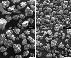
In polymer characterization, Scanning Electron Microscopy (SEM) is invaluable for examining surface topography, morphology, and composition. It allows researchers to visualize and analyze features at the micro and nanoscale, providing crucial insights into polymer structure and properties. The versatility and capabilities of SEM have made it an essential tool in materials science and polymer research, enabling advancements in various fields of study and industrial applications. SEM utilizes a focused beam of electrons (typically up to 40 keV) to scan a specimen’s surface and creates magnified images (Bogner et al., 2007; Goldstein et al., 2017). Some examples of SEM images of superabsorbent polymers are shown in Figure 1 (which provides examples of SEM images of superabsorbent polymers (SAPs), demonstrating their diverse morphologies, including irregular fragmented particles, spherical granules, aggregated clusters, and porous structures, with scales emphasizing feature sizes from 50 μm to 500 μm; these materials exhibit swelling as they absorb liquid, significantly increasing in size due to their high water retention capacity).

Figure 1. examples of SEM images of superabsorbent polymers (Jensen, O. M., 2011).
The development of SEM can be traced back to the early 20th century, rooted in the exploration of electron optics. The first “scanning microscope” was built by Knoll in 1935, though its resolution was limited to about 100 μm due to the lack of demagnifying lenses. In 1938, von Ardenne articulated the theoretical principles of the scanning microscope as we know it today. The first true SEM was developed in 1942 by Zworykin, who demonstrated that secondary electrons could provide topographic contrast (Bogner et al., 2007; Goldstein et al., 2017).
Subsequent developments included Oatley’s work in 1948, Smith in 1956, and the creation of the Everhart-Thornley detector in 1960. These advancements culminated in the SEM V prototype in 1963, which led to the first commercial SEM in 1965 – the Cambridge Scientific Instruments Mark I “Stereoscan” (Bogner et al., 2007).
Scanning Electron Microscopy (SEM) operates by directing a focused electron beam onto the surface of a specimen, scanning it in a raster pattern. The interaction generates various signals, including secondary electrons, backscattered electrons, and characteristic X-rays, which are collected to form images or analyze the sample surface. Backscattered electrons (BSEs), which retain much of their original energy after being deflected by atomic electric fields, and secondary electrons (SEs) are low-energy electrons emitted from the surface after being displaced by the beam. These electron interactions form the basis of the detailed imaging and analysis capabilities of SEM (Bogner et al., 2007; Goldstein et al., 2017).
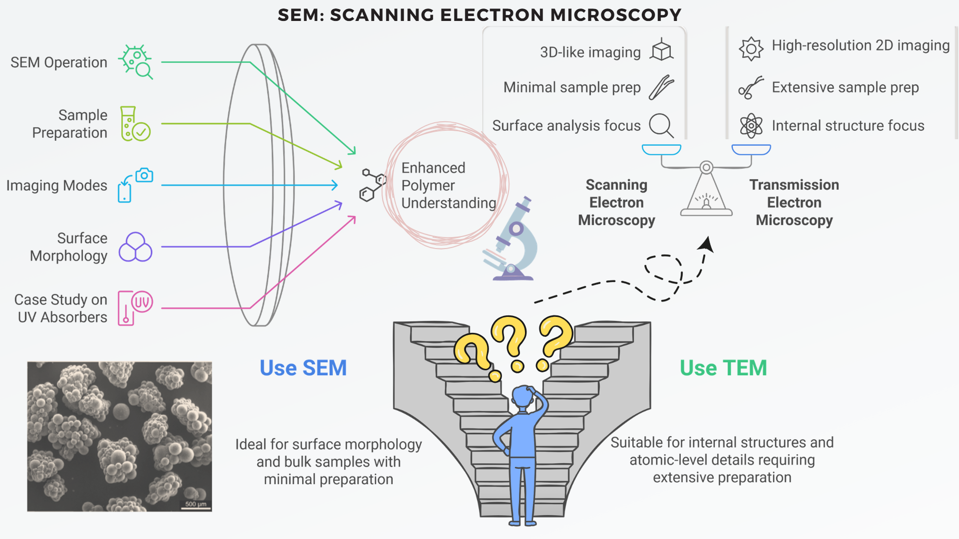
SEM uses electron beams which is similar to Transmission Electron Microscope (TEM), but unlike TEM, which requires extremely thin specimens, SEM can image thicker samples (up to ~mm), making it particularly useful for examining bulk materials. While SEM offers lower magnification than TEM, it provides valuable three-dimensional information about specimen surfaces over a wide range of length scales (Bogner et al., 2007).
In this chapter more information will be given on how SEM works, what is the difference between the SEM and TEM method, sample preparation, imaging modes, application of SEM in polymer characterization and a review will be given on an article that used this method to study Modifications of Polymers through the Addition of Ultraviolet Absorbers to Reduce the Aging Effect of Accelerated and Natural Irradiation,” focuses on the use of ultraviolet (UV) absorbers to enhance the photostability of polymers, particularly poly(vinyl chloride) (PVC) and polystyrene (PS)
How SEM Works
In the SEM, a finely focused beam of energetic electrons is generated and directed onto a sample. This beam interacts with the sample’s surface, primarily through elastic and inelastic scattering (Elastic scattering changes the direction of the electron without energy loss, while inelastic scattering results in energy transfer to the sample). Elastic scattering alters the direction of electrons without significant energy loss, while inelastic scattering results in energy transfer to the sample, generating signals such as secondary and backscattered electrons. Secondary electrons (SEs) are emitted when incident electrons transfer energy to loosely bound electrons in the sample, ejecting them near the surface. They are crucial for surface topography imaging due to their shallow escape depth. Backscattered electrons (BSEs), in contrast, are produced via elastic collisions and provide compositional contrast by reflecting differences in atomic numbers (Goldstein et al., 2017).
SEM achieves high-resolution imaging by controlling beam parameters and utilizing specific detectors. SEs are used to reveal surface topography with fine detail, while BSEs enhance compositional contrast. The resolution and imaging quality depend on factors such as beam energy, working distance, and the precision of the electron optics (Goldstein et al., 2017).
Comparison to TEM method
Transmission Electron Microscopy (TEM) is a powerful technique that uses a high-energy electron beam transmitted through an ultra-thin sample to produce detailed images, enabling the examination of internal structures and atomic-scale features.
The choice between SEM and TEM for polymer sample imaging depends primarily on the expected feature size, with SEM being suitable for features over 100 nm and TEM preferred for smaller structures, though the latter requires more complex sample preparation (Raja & Barron, 2024).
Here’s a comparison of TEM and SEM presented in a table format:
| Aspect | SEM (Scanning Electron Microscopy) | TEM (Transmission Electron Microscopy) |
| Principle of Operation | Scans the surface of a sample with a focused electron beam; produces signals like secondary and backscattered electrons. | Transmits a high-energy electron beam through a thin sample; analyzes transmitted and diffracted electrons. |
| Imaging | 3D-like surface images; excellent depth of field for morphology and texture. | 2D images of internal structures; very high magnifications and resolutions. |
| Resolution | 1–10 nm, depending on conditions and equipment. | Sub-nanometer resolution, capable of atomic-scale imaging. |
| Sample Preparation | Minimal; may require a conductive coating for non-conductive samples. | Extensive; sample must be ultra-thin (<100 nm). |
| Sample Thickness | Analyzes bulk samples without strict thickness constraints. | Requires thin samples for electron transmission. |
| Applications | Surface morphology, topography, fracture analysis, and compositional contrast. | Crystallography, internal structure, defects, and high-resolution imaging. |
| Electron Beam Energy | Operates at low energies (0.1–30 keV), suitable for surface studies. | Uses high energies (60–300 keV) for penetration of thin samples. |
| Detectors and Signals | Detects secondary electrons, backscattered electrons, and X-rays. | Detects transmitted electrons, scattered electrons, and diffraction patterns. |
| Instrumentation Size | Compact and user-friendly. | Larger, more complex, and requires greater maintenance. |
Take a look at this interactive video about SEM and TEM:
Sample Preparation for Polymer Analysis
Preparing polymers for SEM often involves techniques to avoid charging effects and ensure clear imaging. This may include cutting, polishing, and coating the sample with a conductive layer like gold or carbon. Proper preparation ensures accurate imaging of surface morphology and eliminates artifacts that could arise from the polymer’s non-conductive nature (Goldstein et al., 2017).
Conductive samples typically do not require extensive preparation other than grounding. Non-conductive samples, such as polymers, need a conductive coating to prevent the accumulation of charge from the electron beam. This coating must be applied thinly and evenly, especially for samples with intricate surface structures (Goldstein et al., 2017).
Note that samples coated with conductive layers for SEM imaging cannot typically be reused, as the coating alters their original surface properties permanently. SEM samples should generally fit within the microscope’s chamber, with typical dimensions being a few millimeters to a few centimeters in diameter and thickness. Specific size constraints depend on the SEM model and stage configuration.
Sputter coating is the process of depositing a conductive material, such as gold or carbon, onto the sample’s surface in a controlled manner. Mounting involves attaching the sample to a holder using conductive adhesives to establish a path for electron discharge. Careful handling ensures the sample remains clean and properly aligned for imaging (Goldstein et al., 2017).
Polymer samples can exist in various forms, including both liquid and powder states, depending on their specific properties and intended applications. However, for SEM imaging, solid forms are typically used. Here’s how polymer samples are usually prepared:
Imaging Modes and Their Uses in SEM
Secondary electron imaging emphasizes surface details and is ideal for topographic studies. Backscattered electron imaging focuses on compositional contrast and is effective for distinguishing materials of varying atomic numbers. Energy-dispersive X-ray spectroscopy (EDS) allows elemental mapping by detecting characteristic X-rays emitted during electron interactions (Goldstein et al., 2017).
Applications of SEM in Polymer Characterization
SEM is extensively used for analyzing polymers due to its ability to examine surface features and defects with high precision. It aids in understanding polymer morphology, structural characteristics, and material interfaces, making it a valuable tool in studying the effects of processing conditions and surface modifications (Goldstein et al., 2017).
SEM can be used to:
- Analyze Fracture Surfaces and Defects: Fracture surfaces of polymers reveal information about failure mechanisms, such as brittle or ductile fracture. SEM also identifies defects like voids or inclusions, which can impact material performance
- Studying Coatings, Layering, and Adhesion Propertie: SEM can investigate multi-layered structures, including coatings and adhesives. By examining cross-sections, SEM evaluates the uniformity, thickness, and adhesion quality of coatings (Goldstein et al., 2017).
Interpreting SEM Images
Interpreting Scanning Electron Microscopy (SEM) images is a crucial skill for researchers working with polymers, microstructures and nanomaterials. SEM provides valuable information about surface morphology, particle size, and material distribution at the micro and nanoscale.
When analyzing SEM micrographs, it is important to first consider the scale bar, which indicates the size of the features being observed. This allows for accurate measurement of structures such as fibers, particles, or pores. Pay attention to the overall distribution and arrangement of the material, noting any patterns or irregularities. Surface texture can reveal important details about the material’s properties, so observe whether surfaces appear smooth, rough, or porous. For fibrous materials, examine the diameter, length, and orientation of individual fibers. In cross-sectional images, look for information about internal structures or layering. The brightness and contrast in SEM images can also provide insights into the composition, as heavier elements typically appear brighter. By carefully examining these aspects, researchers can extract valuable data about their samples’ morphology, size distribution, and structural characteristics.
Peered Review Article
El-Hiti et al. in 2022, addressed the issue of polymer degradation caused by ultraviolet (UV) radiation exposure, particularly in poly(vinyl chloride) (PVC) and polystyrene (PS). They investigated various UV absorbers, including Schiff bases, polyphosphates, and metal complexes, to enhance the photostability of these polymers, as these additives are incorporated into polymer films to reduce the degradation caused by UV radiation
The Scanning Electron Microscopy (SEM) method played a crucial role in this research:
- Surface Morphology Analysis: SEM was used to examine the surface characteristics of irradiated polymer films, both with and without UV absorbers.
- Degradation Assessment: The technique helped visualize the extent of polymer degradation by revealing surface irregularities, cracks, and other morphological changes.
- Comparative Studies: SEM images allowed researchers to compare the effectiveness of different UV absorbers by observing the degree of surface damage in treated and untreated samples.
- Quantitative Analysis: The roughness factor (Rq) of polymer surfaces was determined using SEM data, providing a quantitative measure of the UV absorbers’ effectiveness.
- Mechanism Insights: SEM observations contributed to understanding the mechanisms by which UV absorbers protect polymers from photodegradation.
The SEM (Scanning Electron Microscopy) images in this article provide valuable insights into the surface morphology of polymer films before and after the addition of UV absorbers. Let’s compare two key images:

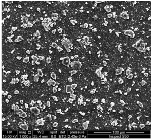
Figure 2. SEM image of the surface of an irradiated PVC film blended with a Schiff base of melamine.

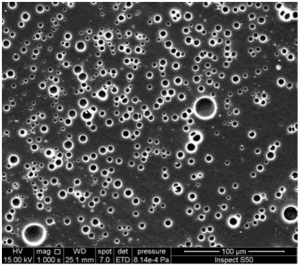
Figure 3. SEM image of the surface of an irradiated PS film blended with a Schiff base of biphenyl-3,3′,4,4′-tetraamine.
Figure 2 shows the SEM image of an irradiated PVC film blended with a Schiff base of melamine. The surface morphology reveals a distinct ice-cube-like particle structure. This unique formation is likely due to the following factors:
- Slow elimination of volatiles and hydrogen chloride
- Crosslinking reactions within the polymer matrix
- Interaction between the melamine Schiff base and the PVC chains
The ice-cube-like particles appear to be uniformly distributed across the surface, indicating a homogeneous dispersion of the additive within the polymer film. This structure may contribute to enhanced UV protection by scattering incident light and providing a physical barrier against degradation.
Figure 3 presents the SEM image of an irradiated polystyrene (PS) film blended with a Schiff base of biphenyl-3,3′,4,4′-tetraamine. The surface morphology exhibits remarkable features:
- Spherical pores: The image shows well-defined spherical pores distributed across the surface.
- Embedded ellipsoid structures: Alongside the spherical pores, there are embedded ellipsoid structures.
- Pore size: The diameter of these pores ranges from 3.4 to 4.3 μm.
This porous structure is likely a result of:
- Effective light absorption by the UV absorber
- Phase separation during the film formation process
- Controlled evaporation of solvents
The formation of these ball-like pores may enhance the UV-protective properties of the film by:
- Increasing the surface area for light scattering
- Creating a tortuous path for UV radiation
- Potentially trapping and dissipating harmful UV energy
These SEM images demonstrate the significant impact of UV absorber additives on the surface morphology of polymer films. The unique structures formed can contribute to improved photostability and may offer additional functional properties to the materials.
The study demonstrated that the addition of UV absorbers significantly reduced the surface roughness of irradiated polymer films, with some additives decreasing the roughness factor by up to 27-fold. This research provides valuable insights into improving the longevity and performance of polymers exposed to UV radiation, which has important implications for various applications in industries such as construction, packaging, and automotive.
References
Jensen, O. M. (2011). Water absorption of superabsorbent polymers in a cementitious environment. In International Conference on Advances in Construction Materials through Science and Engineering 2011. Rilem publications.
Bogner, A., Jouneau, P. H., Thollet, G., Basset, D., & Gauthier, C. (2007). A history of scanning electron microscopy developments: Towards “wet-STEM” imaging. Micron, 38(4), 390-401.
Goldstein, J. I., Newbury, D. E., Michael, J. R., Ritchie, N. W., Scott, J. H. J., & Joy, D. C. (2017). Scanning electron microscopy and X-ray microanalysis. Springer.
Raja, P. M. V., & Barron, A. R. (n.d.). SEM and its Applications for Polymer Science. In A. R. Barron (Ed.), Physical Methods in Chemistry and Nano Science. LibreTexts. https://chem.libretexts.org/Bookshelves/Analytical_Chemistry/Physical_Methods_in_Chemistry_and_Nano_Science_(Barron)/09:_Surface_Morphology_and_Structure/9.03:_SEM_and_its_Applications_for_Polymer_Science
El-Hiti, G. A., Ahmed, D. S., Yousif, E., Al-Khazrajy, O. S., Abdallh, M., & Alanazi, S. A. (2021). Modifications of polymers through the addition of ultraviolet absorbers to reduce the aging effect of accelerated and natural irradiation. Polymers, 14(1), 20.

