14 The Basics of Atomic Force Microscopy in Surface Morphology
skim84
Chapter Overview
- Introduction
- General set up of AFM
- AFM Scanning mode
- Static mode
- Dynamic mode
- Sample Preparation
- Imaging of Surface Topography
- Part 1: Research Application of Using AFM
- Part 2: Research Application of Using AFM
- Conclusion
Graphical Abstract:
1. Introduction
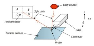
Figure 1. General Structural AFM Probe in contact with the sample surface [2]
Atomic Force Microscope is well known as AFM and it evolved from previous microscopes such as scanning force microscope (SFM) to cover the limitations. AFM was invented in 1986. AFM allows for the surface topography of the sample surface to be obtained by detecting the force between the tip of the cantilever and the sample surface. It can measure tip-sample force detection of conductive and non-conductive samples. The probes of the AFM are in diverse structures, but mainly from silicon or silicon nitride. [1], [2], [3]
In addition to analyzing surface morphology with nanometer-scale precision, atomic force microscopy (AFM) has enriched the understanding and analysis of surface characteristics of different subjects. The subjects that the AFM acts for strong inputs can range from material science to biology.
The AFM operation is based on force detection from a tip mounted on a flexible cantilever. The force detection allows for generating highly detailed topographical maps and mechanical properties measurement of sample surfaces.
One of the advantages of AFM is its ability to obtain data from conductive and non-conductive samples. This allows for a wide range of applications and diverse samples. In addition, AFM allows for generating three-dimensional images of surface features in different modes. In this chapter, the static/contact mode and dynamic mode will be focused. The significance will be explored in addition to the advantages and disadvantages of each mode. Therefore, a more enriched understanding of material properties at the atomic and molecular level will be obtained.
The use of AFM is non-destructive and allows for observing changes in surface morphology or characteristics over time. In the battery research field, AFM allows for visualization of electrode degradation which connects to the relationships between surface morphology and performance.
This chapter will provide insight into the fundamental understanding of AFM and its application to surface morphology studies. The overview of fundamental operations, different modes, and sample preparation will be explained. [3], [4]
2. General Set Up of AFM
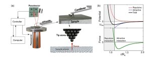
Figure 2. Interaction Force between Sample Atom and Cantilever Atom [4]
AFM image is based on attractive and repulsive interaction with the sample which is composed of the following parts: cantilever with a sharp tip, detection system associated with the cantilever’s bending action, movement system that allows to scan the sample surface, graphical visualization system, feedback control to apply force. [4]
One of the Critical factors for general AFM set up are stability of the sample surface which focuses on limiting contamination layers. Force measured between the tip and the sample surface can be distorted with contaminated particles. Reduction in the vibrational environment is also critical; it can interrupt the sensitivity of the cantilever. [3]
During the scanning process, the interaction force between the tip and the sample surface is measured through the bending of the cantilever. In detail, the length of the cantilever is about 200 to 400 um, and the width of 20 to 40 um. The tip attached to the edge of the cantilever is known as “V-shaped” with a radius ranging from 15 to 20 nm. This action allows the laser beam/photodiode to change from its initial state. In response, the signal is transferred to the feedback electronics system. The scanning occurs in three-dimensional space, where the scan can range in y direction up to 100 um, x up to 100 um, and z of 30 um. [4]
3. AFM Scanning Mode
a. Static Mode
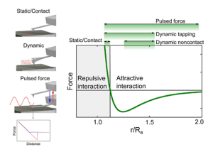
Figure 3. Images of different AFM Operating Mode and Force regions. [3]
Static mode known as contact mode is when the tip is continuously in contact with the sample surface. This model is focused on the repulsive force component where force is applied to the sample surface in the z direction of the cantilever. The surface is scanned while the force is constant at a set limit. This mode is used for flat surfaces and allows for high resolution of images due to continuous contact between the tip and surface. However, the constant set force applied can cause damage to the sample surface. The tip dragged throughout the scanning process, can potentially cause the removal of previously scanned surfaces and cause distortion. Therefore, scanning relatively hard surfaces is recommended. The constant force contact mode also allows for small scan areas. [3], [4]
The constant interaction between the tip and surface allows for highly detailed surface maps and images of hard surface materials. The advantage is for fast data collection but can cause damage to soft surface features. The static mode should be used for material science research fields about films and the microstructure of surfaces. [1],[5],[6]
Contact Mode:
b. Dynamic Mode
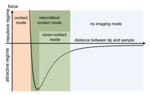
Figure. 4 Force-distance Curve Showing Interaction between The Cantilever Tip and The Sample Surface at Different Operation Modes. [4]
As shown in figure 4, dynamic mode is focused mainly on repulsive regime. Dynamic mode focuses on tapping action and it is a non-contact mode that covers the limitations of static mode. The cantilever will oscillate at a specific frequency which is at its greatest amplitude. Tapping mode allows for irregular contact of the tip and surface which reduces frictional and lateral forces. Therefore, it is more suitable for soft surfaces such as biological sample imaging. The van der Waals force is the dominant force involved during this mode. This allows for tip distance from the surface and less physical contact which will reduce surface distortion compared to static mode. [3],[4]
Additionally, the dynamic mode provides high-resolution images. The field frequencies using this mode are nanoscale topography, polymer films, and biological cells. All subjects are considered delicate materials compared to the samples scanned in static mode. The scanning of delicate materials needs confirmation of a high level of calibration and steady operation to maintain stable oscillation. The factors that can affect imaging are humidity and temperature. [3], [4]
Non Contact Mode:
4. Sample Preparation
Sample preparation is critical for establishing a foundation for accurate AFM measurements and data collection. The sample surface is required to be free from contaminants for accurate imaging. The preparation procedure is dependent on the type of samples. For example, polymer thin films should be produced in the spin coated procedure for having high uniformity. Biological specimens should be mounted with a substrate to prevent moving locations during the image scanning process. [3],[4]
5. Imaging System of Surface Topography
The imaging system is composed of a cantilever with a tip, a laser to detect cantilever deflection, and a feedback loop that controls the applied force between the tip and the sample. The component that allows surface topography imaging is the piezoelectric actuator. [3],[4]
6. Part 1: Research Application of Using AFM
The research paper is titled “Surface characteristics of 3D printed PEEK polymer using atomic force microscopy”. This paper is about surface characteristics of 3D-printed polyetheretherketone which is a thermoplastic polymer with semi-crystalline properties. It is well known for high strength, and lower thermal conductivity, and used in medical applications for implants and dental prostheses. PEEK material is studied for reducing surface roughness which can be obtained from surface morphology. The surface roughness can be reduced by altering 3D printing parameters such as printing speed and layer height. Four specimens were fabricated for microstructural characteristics analysis. The following figure 5 list details about printing parameters effecting surface micrographs as seen in figure 6.

Figure 5. 3D Printing Parameters for S1, S2, S3, and S4 (S represents Specimen) [5]
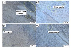
Figure 6. Surface Micrographs of Specimen 1 (a), S2 (b), S3 (c), and S4 (d) [5]
Sample preparation involved printed PEEK samples with layer heights ranging from 0.10 to 0.15 mm and printing speeds of 20 to 25 mm/s. The AFM allowed for surface roughness scanning around adhesion and interlayer bonding areas. Specimen S3 which was printed at 0.15mm layer height and 20 mm/s showed the lowest surface roughness of 0.017 um. Lower surface roughness indicated fewer defects and stronger adhesion properties for optimization of sample parameters. The detailed 2D and 3D view of specimen 3 can be observed in figure 7.
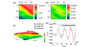
Figure 7. Surface Roughness of Specimen 3. Topography 2D (a), Deflection 2D (b), Roughness 3D (c), Roughness profile (d). [5]
There was a direct relationship between printing parameters and surface morphology. The optimization of those parameters allows samples to exhibit higher mechanical properties. These results can be applied in biomedical fields for application for 3D printed PEEK components and expanded for future research to chemical composition relationships. [5]
7. Part 2: Research Application of Using AFM
The research paper is titled “Characterization of polyamide thin films by atomic force microscopy “. This paper is about the analysis of thin polyimide films on molecular layer deposition (MLD) with interfacial polymerization (IP) techniques. The surface of the reverse osmosis desalination membrane exhibits surface roughness. The quantification of these properties (surface roughness and mechanical properties) is analyzed through the use of AFM at dry and hydrated states.
The sample preparation was performed through the fabrication of MLD polyamide films with controlled thickness and IP films. The films were analyzed through AFM in different environmental conditions such as hydration and chlorination to measure surface roughness and modulus. As a result, MLD films resulted in greater smoothness, higher elastic modulus, and higher density than IP films. From the different environmental conditions, MLD films resulted in stronger mechanical integrity than IP films under stress.
In conclusion, MLD films are suitable for application for stronger mechanical properties and resistance to environmental degradation. The lower roughness and higher modulus indicate higher durability. Therefore this study allowed for obtaining properties of thin films through deposition techniques (MLD). [6]
8. Conclusion
Atomic Force Microscopy (AFM) is an effective tool for surface morphology studies in diverse research fields with depths in the nanoscale. The operational modes such as static and dynamic offer the most suitable testing for different sample types which can range from soft to hard surfaces. The surfaces could be solid-like materials, polymer films, and very fragile biological specimens. The sample preparation allows for more accurate and detailed imaging results and increases the reliability of the obtained measurements. As the research technology advances, the application of AFM will be more broad and could result in significant findings of material properties in nanoscale. [3],[4]
